



Post Date : Monday, July 08, 2024
3D Visualization Holds Key to Future Chip Designs

At this week's Design Automation Conference, Ansys is showcasing how NVIDIA Omniverse and Modulus are revolutionizing simulation workflows, offering insights into the future of chip design.
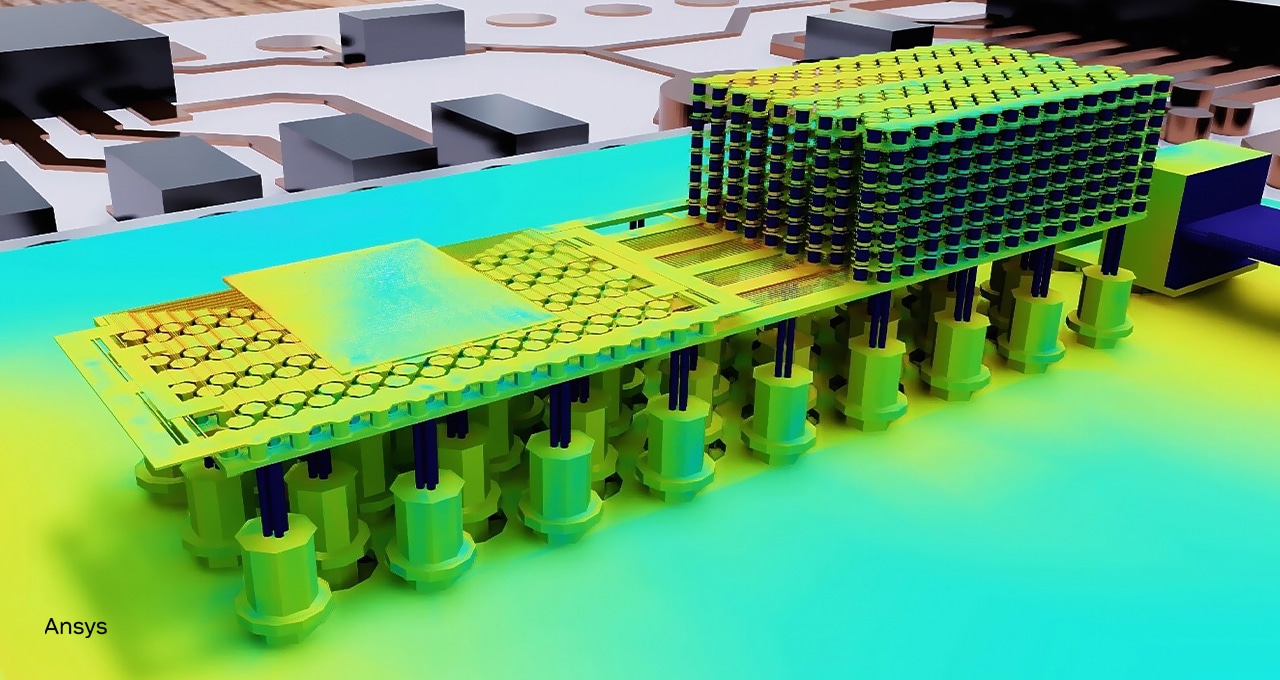
Three-dimensional integrated circuits (3D-ICs) represent a groundbreaking advancement in semiconductor design. By vertically stacking chips, manufacturers can create a compact structure that significantly enhances performance without increasing power consumption. However, this increased density introduces complex challenges, particularly in managing electromagnetic and thermal stresses. To address these issues, advanced 3D multiphysics visualizations are becoming essential in both the design and diagnostic processes.
At the Design Automation Conference, a global event highlighting the latest developments in chips and systems, Ansys—known for its engineering simulation and 3D design software—will demonstrate how it leverages NVIDIA technology to tackle these challenges and build the next generation of semiconductor systems.
To facilitate 3D visualizations of simulation results, Ansys utilizes NVIDIA Omniverse, a comprehensive platform comprising APIs, software development kits, and services. This platform enables developers to seamlessly integrate Universal Scene Description (OpenUSD) and NVIDIA RTX rendering technologies into existing software tools and simulation workflows. By doing so, Omniverse powers the visualization of 3D-IC results from Ansys solvers, allowing engineers to assess phenomena such as electromagnetic fields and temperature variations, ultimately optimizing chip design for faster processing, increased functionality, and improved reliability.
With Ansys Icepak integrated into the NVIDIA Omniverse platform, engineers can simulate temperatures across a chip according to various power profiles and floor plans. Identifying hot-spots on the chip can lead to improved chip designs and more effective auxiliary cooling devices. However, these 3D-IC simulations are computationally intensive, often limiting the number of simulations and design points that users can explore.
To overcome these limitations, Ansys is exploring the acceleration of simulation workflows using AI-based surrogate models developed with NVIDIA Modulus. Modulus is an open-source AI framework designed for building, training, and fine-tuning physics-ML models at scale using a simple Python interface. By employing the NVIDIA Modulus Fourier neural operator (FNO) architecture, which parameterizes solutions for partial differential equations, Ansys researchers have created an AI surrogate model capable of efficiently predicting temperature profiles for any given power profile and floor plan. This model offers near real-time results at significantly reduced computational costs, enabling Ansys users to explore a wider design space for new chips.
Following a successful proof of concept, Ansys plans to integrate these AI surrogate models into its next-generation RedHawk-SC platform using NVIDIA Modulus. As more surrogate models are developed, Ansys aims to enhance model generality and accuracy through in-situ fine-tuning. This will enable RedHawk-SC users to benefit from faster simulation workflows, access to a broader design space, and the ability to refine models with their own data, fostering innovation and safety in product development.
For those interested in witnessing the joint demonstration of 3D-IC multiphysics visualization using NVIDIA Omniverse APIs, Ansys will be presenting at the Design Automation Conference, running from June 23-27 in San Francisco at booth 1308. Additionally, the presentation will be featured at the Exhibitor Forum, providing a deeper look into how these advancements are shaping the future of chip design.
The collaboration between Ansys and NVIDIA highlights the critical role of 3D visualization in the future of semiconductor design. By leveraging advanced AI and visualization technologies, these companies are paving the way for more efficient, reliable, and innovative chip designs, addressing the complex challenges posed by increasingly dense 3D-ICs. This partnership not only enhances current capabilities but also sets the stage for continued advancements in the field of semiconductor engineering.